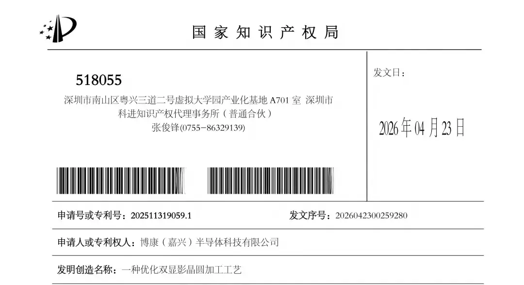
Recently, the invention "An Optimized Double-Development Wafer Processing Method," independently developed by Boncom (Jiaxing) Semiconductor Technology Co., Ltd., passed the rigorous review of the China National Intellectual Property Administration and was officially granted a national invention patent.
Double-development is a critical process step in wafer manufacturing. This patented technology introduces improvements and optimizations based on actual production processes, effectively enhancing process stability and production efficiency while further strengthening Boncom's technological footprint in wafer processing.
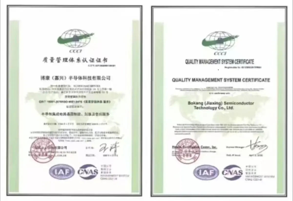
Boncom has long been committed to a technology-driven, innovation-led strategy, continuously advancing semiconductor process R&D and building deep technical expertise. The grant of this patent is a clear testament to the company's accumulated capabilities and innovative strength.
Moving forward, Boncom will continue to deepen its focus on the semiconductor field, driving technological iteration and core process refinement. The company is dedicated to transforming R&D innovations into tangible outcomes, empowering the semiconductor industry with sustainable, high-quality momentum.
Building growth on a solid technology foundation, and advancing with action on a long-term journey. As the industry enters a new cycle of development, Boncom remains true to its innovation-driven mission, committed to process breakthroughs and technical excellence — moving forward steadily on the path to high-quality semiconductor development, and continuously injecting fresh innovation and core energy into the evolution of the industry.
关注我们