Skip to content
  • Home
  • About
  • Solutions

    Wafer Fabrication

    Advanced Nodes. Quality Foundry.

    Packaging Services

    Precision Packaging. Superior Interconnect.

    Specialty Technologies

    Differentiated. Deep Customization.

    Design Support

    Full Testing. Quality Assured.

  • News
  • Quality
  • Contact
  • Join Us
  • Language
    • China - 简体中文
    • Global - English

News

Newsnioxe_admin2026-05-22T16:18:30+08:00
  • Milestone Achieved: Boncom Technology Center Recognized as Jiaxing Municipal High-Tech R&D Center

    2026/7/10
  • Boncom NIP2 Process – Ready to Launch!

    2026/5/14
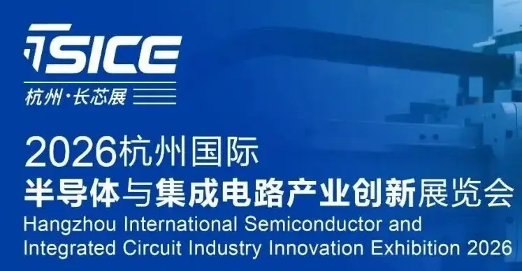
  • Exhibition Invitation | Boncom Invites You to SICE 2026 in Hangzhou & Zhejiang (Haining) Semiconductor Equipment & Materials Expo in May

    2026/4/29
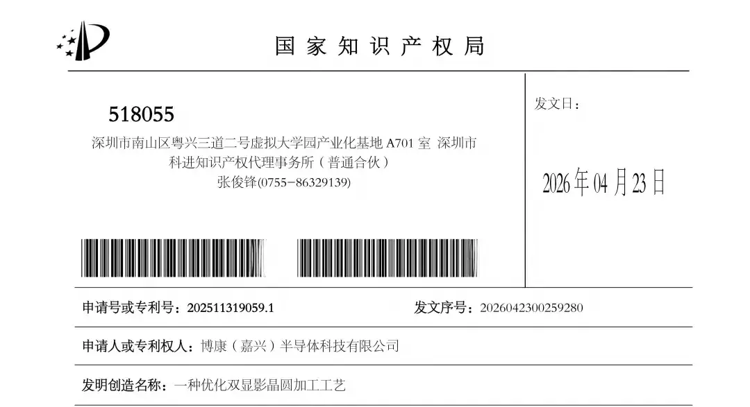
  • Technology Breakthrough | Boncom Granted National Invention Patent for Self-Developed Process

    2026/4/27
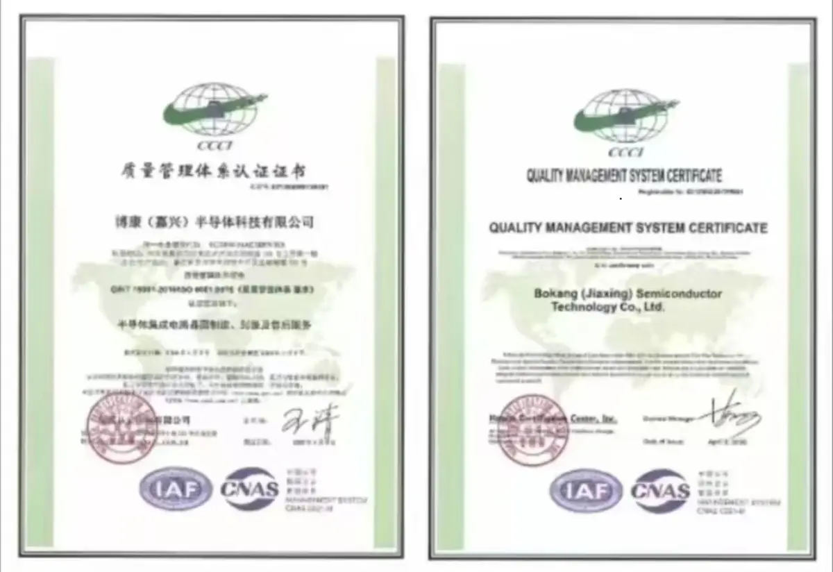
  • Milestone | Boncom Achieves ISO 9001 Quality Management System Certification

    2026/4/10
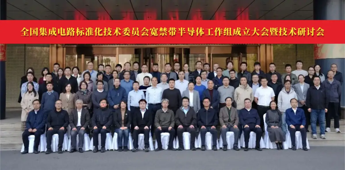
  • Zhang Bo, Chairman of Boncom, Joins First National IC Standardization Committee's Wide Bandgap Semiconductor Working Group as Member

    2026/4/1
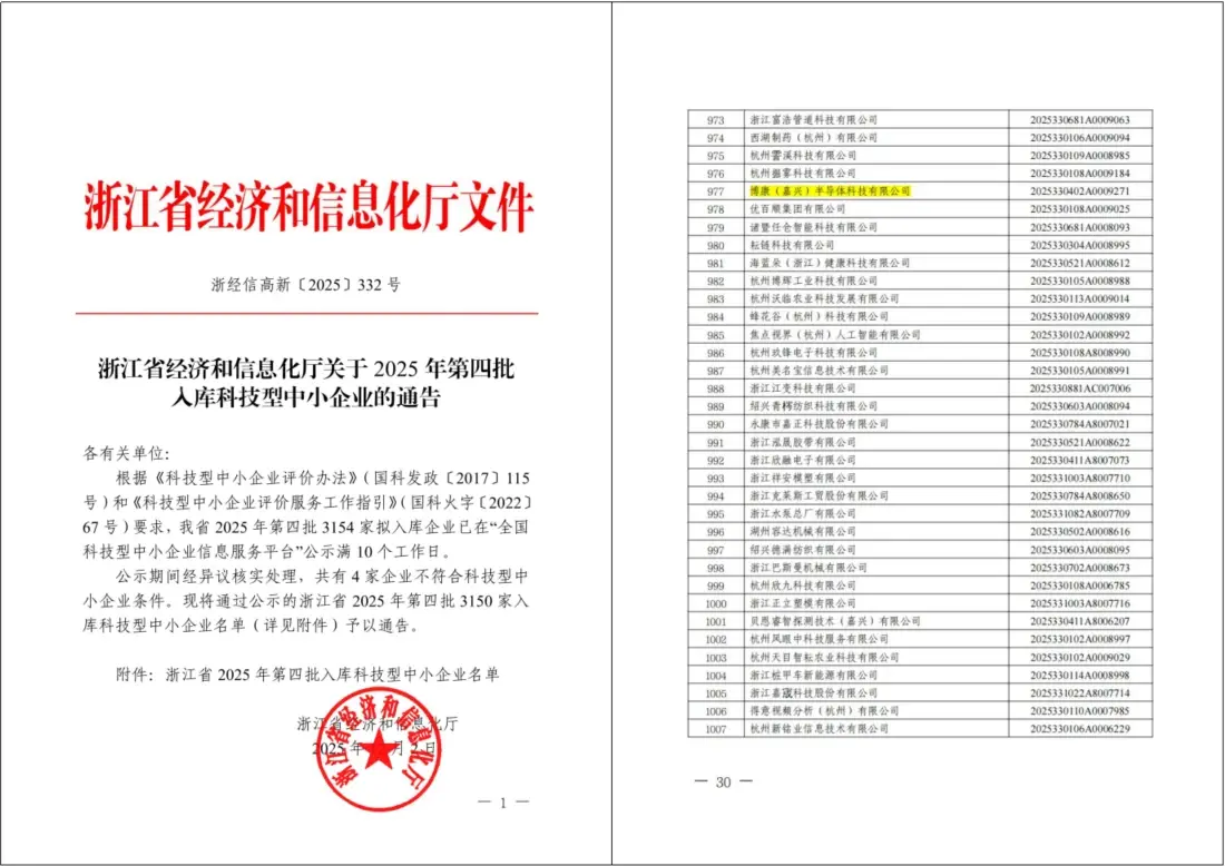
  • Great News! Boncom Semiconductor Selected as One of Zhejiang Province's 2025 Fourth Batch of National-Level Tech-oriented SMEs

    2025/12/5
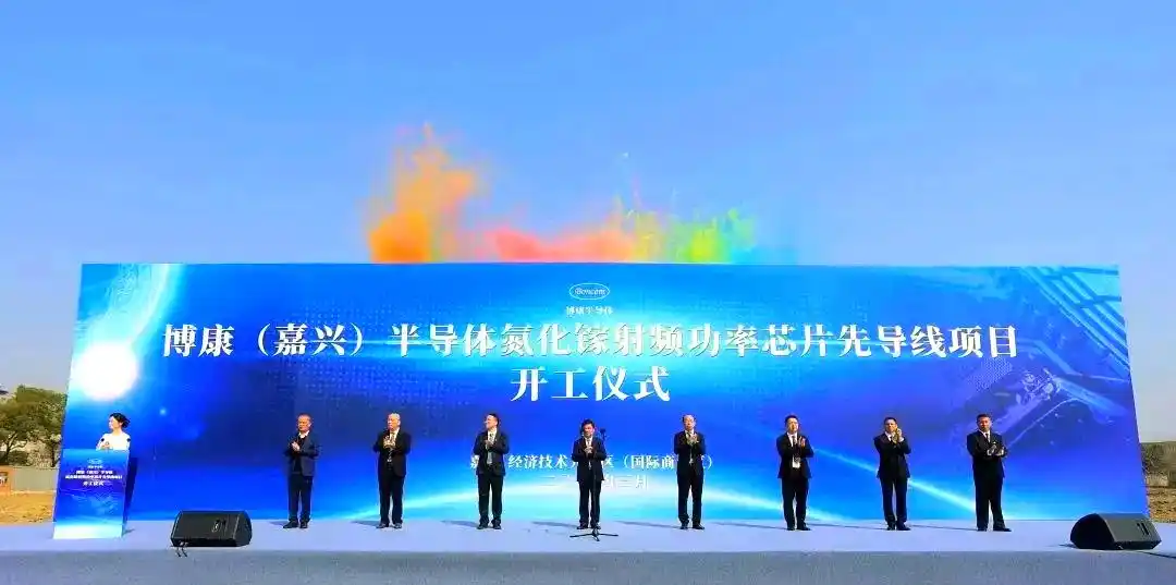
  • Boncom Breaks Ground on GaN RF Power Chip Pilot Line Project in Jiaxing with Total Investment of Approximately RMB 600 Million

    2023/3/1

Where the mind goes, our chips follow.

Contact

No. 108, Zhaohui Road, Nanhu District, Jiaxing City, Zhejiang Province, China
Tel : 0573-82588518
E-Mail : information@boncom-semi.com

Solutions
  • Wafer Fabrication
  • Packaging Services
  • Specialty Technologies
  • Design Support
Follow Us

Copyright © 2022- Boncom (Jiaxing) Semiconductor Technology Co., Ltd. All rights reserved.

Page load link
Go to Top